Research progress of large size SiC single crystal materials and ...
2023.1.24 Silicon carbide (SiC) is a wide band gap semiconductor, and because of it has high thermal conductivity and excellent electronic properties, SiC is widely used in
Charlar en Línea
Automatic crushing device for polycrystalline silicon
2019.12.31 4. The automatic crushing device for the polycrystalline silicon according to claim 3, wherein the surface of the toothed structure is sprayed on the
Charlar en Línea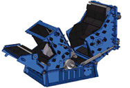
(PDF) Tailored Polycrystalline Substrate for SmartSiCTM Substrates ...
2023.6.6 Silicon Carbide (SiC) Power Devices have emerged as a breakthrough technology for a wide range of applications in the frame of high-power electronics,
Charlar en Línea
Molecular dynamics study on grinding mechanism of
2022.12.1 In this paper, several polycrystalline silicon carbide models are generated based on Voronoi method, and then simulated by molecular dynamics
Charlar en Línea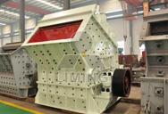
机械工程学报-., 第卷, 第期
多晶碳化硅陶瓷磨削裂纹损伤形成机理研究 [J]. 机械工程学报, 2022, 58 (13): 307-320. DAI Jianbo, SU Honghua, WANG Zhongbin, DING Wenfeng, FU Yucan, CHEN Jiajia.
Charlar en Línea
High-quality grinding of polycrystalline silicon carbide
2004.1.1 The objective of this study was to develop high-quality grinding protocols for polycrystalline silicon carbide spherical surfaces in order to achieve nanometre
Charlar en Línea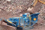
Polycrystalline silicon carbide as a substrate material for
2006.4.25 The in-use adhesion characteristics of polycrystalline cubic silicon carbide (poly-SiC) films when used as a substrate material in MEMS applications are
Charlar en Línea
Polycrystalline silicon carbide for surface micromachining IEEE ...
Abstract: Polycrystalline silicon carbide (poly-SiC) films have been deposited on polysilicon-coated, 4-inch silicon wafers in an atmospheric pressure chemical vapor
Charlar en Línea
Robust Polycrystalline 3C-Sic-on-Si Heterostructures with Low CTE ...
Abstract: In this paper we present for the first time polycrystalline cubic silicon carbide on monocrystalline silicon (3C-SiC-on-Si) heterostructures with very low coefficient of
Charlar en Línea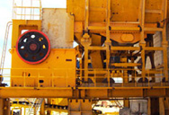
Polycrystalline silicon chunks and method for producing them
Methods for producing polycrystalline silicon chunks, include the steps of providing a polycrystalline silicon rod, comminuting the polycrystalline silicon rod into cubic chunks, and cleaning the polycrystalline silicon chunks, wherein comminution takes place using a spiked-roll crusher having at least one spiked roll, the spiked roll including W 2 C
Charlar en Línea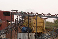
基于分子动力学模拟的纳米多晶 α - 碳化硅变形机制
在考虑晶界和温度效应影响的条件下,基于分子动力学法使用Vashishta势函数研究多晶 -碳化硅基体在纳米压痕作用下的塑性变形机制,分析载荷位移曲线并通过识别变形结构描述了变形区域中的原子破坏和迁移轨迹变化。. 在下压过程中,因接触载荷不断增大在 ...
Charlar en Línea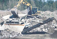
Polysilicon Grinder - Modern Process Equipment
MPE is the undisputed leader in grinding equipment for carbon, offering the most accurate particle size distributions at the highest capacities over any competitor. Factors such as roll speed ratios, corrugations, grinder stage
Charlar en Línea
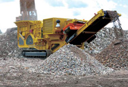
Supply Polycrystalline silicon jaw crusher Wholesale Factory
Polycrystalline silicon jaw crusher Manufacturers and Factory. ... Tungsten carbide cold heading die for punching mould tool parts. Wire drawing die is a very important con. Customized tungsten melting crucible. Tungsten crucible is also know as tungst. Wear plate and ring for concrete pump. 1.
Charlar en Línea
Polycrystalline SiC growth and characterization - ScienceDirect
2004.11.15 Different gas mixtures ratios were used in order to reach the optimal deposition conditions. Fig. 1 exhibits micro-Raman spectra of silicon carbide films deposited for 30 min using a carbon-silicon ratio varying from 1 to 9, while other parameters were fixed: temperature 1000 °C, pressure 10 Torr, H 2 flux 1200 sccm. The evolution of
Charlar en Línea
Fabrication and Characterization of 150-mm Silicon-on-Polycrystalline
substrate. The hybrid substrate consists of a silicon device layer, a thin layer of polycrystalline silicon (poly-Si), and polycrystalline silicon carbide (poly-SiC). The cross-section of the hybrid Si-on-poly-SiC substrate is illustrated in Fig. 1. Poly-SiC has high thermal conductivity and semi-insulating proper-
Charlar en Línea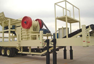
Polycrystalline silicon tungsten carbide jaw plates
HAO Carbide supply various tungsten carbide jaw plates with very good ... Support; Contact us +86-13975383023 Catherine@haocarbide > NEWS. Polycrystalline silicon tungsten carbide jaw plates. Jaw Crusher Tungsten Carbide Jaw Plate Product Description. Jaw crusher models are: PE400×600 jaw crusher, PE500×750 jaw
Charlar en Línea
Simulation Study on Removal Mechanism of Si3N4 Ceramic in
2023.4.21 Hot-pressed Si3N4 ceramic is a kind of high-performance ceramic material, which is widely used in national defense, aerospace, and other professional fields. Aiming at the problem of poor surface quality of Si3N4 ceramic material, the paper carried out a simulation study on the removal mechanism of Si3N4 ceramic by rotary ultrasonic
Charlar en Línea
A molecular dynamics investigation into nanoscale scratching mechanism ...
2018.6.1 Introduction. Ceramic carbides such as silicon carbide (SiC) possess an attractive combination of thermo-mechanical and chemical properties due to their high covalence, making them one of the most useful materials for high-temperature structural applications, such as automotive, aerospace, aviation, laser machine, and nuclear
Charlar en Línea
Reactive ion etching of monocrystalline, polycrystalline, and
1991.3.11 Reactive ion etching of monocrystalline and polycrystalline β‐SiC and hydrogenated amorphous a‐SiC:H in CF 4 /O 2 mixtures was investigated. The a‐SiC:H films, deposited by plasma‐enhanced chemical vapor deposition, had the highest etch rate while monocrystalline β‐SiC had the lowest etch rate at all compositions of the CF 4 /O 2
Charlar en Línea
单晶六方SiC和多晶化学气相沉积SiC的常温辐照肿胀差异性
The difference in swelling behavior between monocrystalline and polycrystalline SiC is experimentally investigated by heavy ion irradiation at room temperature (RT). In this work, single crystal hexagonal (6H) SiC and polycrystalline chemically vapor-deposited (CVD) SiC are irradiated by 1.5 MeV Si ions with the fluences of 11014-21016 cm-2 and 11015
Charlar en Línea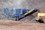
Development of metal-recycling technology in waste crystalline-silicon
2023.5.6 Polycrystalline-silicon solar cells are similar in size to monocrystalline-silicon solar cells, ... Granata et al. used two different types of crusher for coarse crushing and fine crushing of waste solar ... A silicon carbide-based highly transparent passivating contact for crystalline silicon solar cells approaching efficiencies ...
Charlar en Línea
机械工程学报-., 第卷, 第期
Research on the Crack Damage Formation Mechanisms of Polycrystalline Silicon Carbide Ceramics in Grinding Process DAI Jianbo 1,2, SU Honghua 3, WANG Zhongbin 1,2, DING Wenfeng 3, FU Yucan 3, CHEN Jiajia 4 1. College of Mechanical and Electrical Engineering, China University of Mining and Technology, Xuzhou 221008; 2. Jiangsu ...
Charlar en LíneaWelcome - 臧 航 - 教师个人主页
研究领域. 【主要研究方向】. (1)面对航天航空辐射环境及反应堆环境下半导体材料的辐照效应研究,包含辐照缺陷及损伤的多尺度模拟计算、缺陷对电学性能影响和中子及重离子辐照实验;. (2)面对裂变及聚变环境下核结构材料的辐照效应研究,包含辐照 ...
Charlar en Línea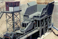
CA2821493A1 - Polycrystalline silicon chunks and method for
Methods for producing polycrystalline silicon chunks, comprising providing a polycrystalline silicon rod, comminuting the polycrystalline silicon rod into cubic chunks, and cleaning the polycrystalline silicon chunks, wherein comminution takes place using a spiked-roll crusher having at least one spiked roll, the spiked roll comprising W2C
Charlar en Línea
A molecular dynamics investigation into nanoscale ... - ScienceDirect
2018.6.1 The silicon carbide has zinc blende structure with 4.35 Å lattice length, where the silicon atoms locate in the corner and surface center and carbon atoms lay on the inside of the crystal cell [24]. The potential function is a physical curve to describe the atoms potential value, which decides the interaction force and energy among the atoms.
Charlar en Línea
Enhanced Ohmic contact via graphitization of polycrystalline silicon ...
Enhanced Ohmic contact via graphitization of polycrystalline silicon carbide F. Liu,1,2 B. Hsia,2 C. Carraro,1,2 A. P. Pisano,1,3 and R. Maboudian1,2,a 1Berkeley ...
Charlar en Línea
Thermodynamic properties of 3C—SiC Semantic Scholar
2013.10.1 The plane-wave pseudopotential approach to density-functional theory (DFT) in the local-density approximation has been applied to investigate a variety of ground-state properties of the 3C, 2H, and 4H polytypes of silicon carbide to obtain lattice-dynamical properties of cubic SiC such as the phonon-dispersion curves. Expand
Charlar en Línea
A molecular dynamics investigation into nanoscale scratching
2018.6.1 DOI: 10.1016/J.COMMATSCI.2018.02.038 Corpus ID: 139155833; A molecular dynamics investigation into nanoscale scratching mechanism of polycrystalline silicon carbide @article{Liu2018AMD, title={A molecular dynamics investigation into nanoscale scratching mechanism of polycrystalline silicon carbide}, author={Yao Liu
Charlar en Línea